Allegro如何创建差分对
2、在弹出的约束管理器对话框中,选择Physical→Net→All Layers→然后选中一个网络按住Ctrl键,选中需要设置为差分对的另一个网络→点击右键Create(创建)→DifferentailPair(差分对)。选中两个Pin Pair,右击→Create(创建)→Match Group...(匹配组)然后为这两个Pin Pair创建匹配组。然后设置好差分对的走线长度误差,设置差分对的
1、点击菜单栏的Setup→Constraints(约束条件)→Electrical(电气)或按快捷键Ctrl+D,如下图所示:
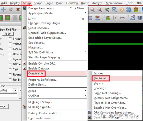
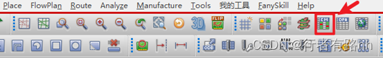
或点击工具栏的约束管理器CM图标,如下图所示:
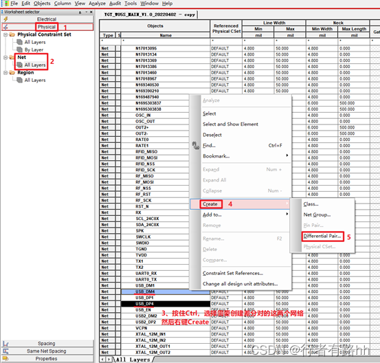
2、在弹出的约束管理器对话框中,选择Physical→Net→All Layers→然后选中一个网络按住Ctrl键,选中需要设置为差分对的另一个网络→点击右键Create(创建)→DifferentailPair(差分对)。点击Differentail Pair(差分对)。如下图所示:
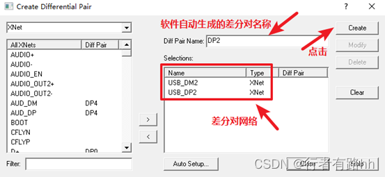
3、跳出下面的对话框,软件会自动生成一个差分对名称,也可自己重新命名。点击Create。关闭对话框
4、差分对即创建成功,如下图
然后给差分对赋予走线约束规则,就完成了对差分对的设置
5、差分对等长
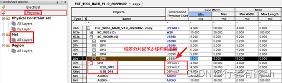
如果网络有Xnet,先创建好Xnet,然后再创建网络的Pin Pair。
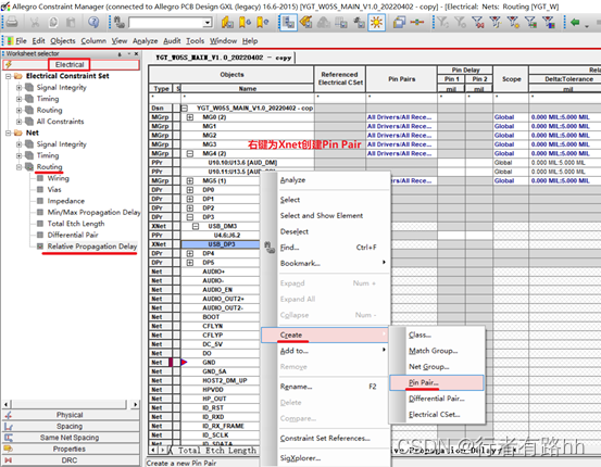
给差分对创建Pin Pair,选择差分对的一个网络右击→Create(创建)→Pin Pair(引脚对),创建好的Pin Pair如下图所示:
选中两个Pin Pair,右击→Create(创建)→Match Group...(匹配组)然后为这两个Pin Pair创建匹配组。
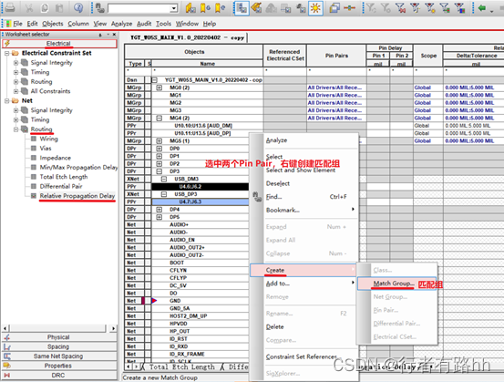
创建好的匹配组如下图所示
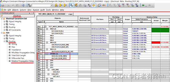
然后设置好差分对的走线长度误差,设置差分对的目标线就可以拉差分对的等长线了。

博主专注职场硬件设计,如果文章对你有帮助,请关注,点赞,收藏。成长路上有前行者。博主将会定期或不定期分享PADS,Allegro设计技巧和经验。
Allegro provides a good and interactive working interface and powerful functions, and its front-end products Cadence, OrCAD, Capture, the combination of high-speed, high-density, multi-layer complex PCB design routing provides the most perfect solution.
Allegro has perfect Constraint Settings, users only need to set the wiring rules according to the requirements, and the design requirements of the wiring can be achieved without violating the DRC when routing, thus saving the tedious manual inspection time and improving the work efficiency!
It can also define parameters such as minimum wire-width or wire-length to meet the needs of today's high-speed circuit board wiring.
Constraint Manger provides a simple interface for users to set and view Constraint declarations.
Its combination with Capture allows E.E. electronics engineers to set up regular data when drawing a circuit diagram and bring it with them to the Allegro working environment, where it can be automatically processed and checked when placing parts and wiring. The empirical values of these regular data can be reused for the same nature of the circuit board design.
In addition to the above functions, Allegro's powerful automatic push and stick line and perfect automatic repair line function provide users with great convenience;
The powerful mapping function can provide multiple users to deal with a complex board at the same time, thus greatly improving the work efficiency.
Or use the optional graph cutting function to cut the circuit board into various blocks, so that each block has a full-time person at the same time to design, to achieve the purpose of the same graph design and can shorten the time course.
After renaming, online interchange and modifying logic during routing, users can easily return to Capture wiring diagram, and update the wiring diagram to Allegro after modification.
Users can also click and modify objects between Capture and Allegro.
有“AI”的1024 = 2048,欢迎大家加入2048 AI社区
更多推荐


 7
7 0
0- 0


 已为社区贡献14条内容

所有评论(0)